| Table of Contents | |
|
Original Article
| ||||||
| Micro and nanofluidic platforms for advanced diagnostics | ||||||
| Elena Angeli1, Valentina Mussi2, Paola Fanzio1, Chiara Manneschi3, Luca Repetto1, Giuseppe Firpo1, Patrizia Guida1, Vincenzo Ierardi1, Andrea Volpe4, Ugo Valbusa1 | ||||||
|
1PhD, Nanomed Labs, Physics Department, University of Genova, L.go Rosanna Benzi, 10, 16132, Genova, Italy.
2PhD, National Research Council, Institute for Complex Systems ISC-CNR, Via del Fosso del Cavaliere 100, 00133 Roma, Italy. 3PhD, National Research Council, Institute of Electronics, Computer and Telecommunication Engineering IEIIT-CNR, Via De Marini 6, 16149 Genoa, Italy. 4BSc, Nanomed Labs, Physics Department, University of Genova, L.go Rosanna Benzi, 10, 16132, Genova, Italy. | ||||||
| ||||||
|
[HTML Abstract]
[PDF Full Text]
[Print This Article]
[Similar article in Pumed] [Similar article in Google Scholar] |
| How to cite this article |
| Angeli E, Mussi V, Fanzio P, Manneschi C, Repetto L, Firpo G, Guida P, Ierardi V, Volpe A, Valbusa U. Micro and nanofluidic platforms for advanced diagnostics. Edorium J Nanotechnol 2014;1:1–7. |
|
Abstract
|
|
Aims:
Sensitivity, selectivity and tunability are keywords to develop effective and reliable diagnostic and bioanalytical tools. In this context, micro and nanofluidic devices constitute a powerful and versatile answer to the growing and urgent demand for innovative solutions. Nevertheless, a precise control of size and functionality of such structures is necessary for ensuring advanced manipulation and sensing capabilities, up to single molecule level.
Methods: We report here on different strategies for the development of micro and nanofluidic platforms for advanced diagnostics based on the exploitation of the elastic properties of deformable materials, and on surface chemical functionalization processes. Results: We demonstrated that applying a macroscopic mechanical compression to elastomeric nanostructures it is possible to increase their confining power and vary the dynamics of DNA translocation process, while the use of the chemical functionalization allows to tune both the size and the functionality of the biosensor. Conclusion: We believe that a smart integration of these two approaches would allow a significant step forward for the fabrication of next-generation lab-on-chip devices for biomedical diagnostic applications. | |
|
Keywords:
Nanochannel, Nanopore, Nanofluidics, Nanofabrication, Biosensing, Polymeric lab-on-chip
| |
|
Introduction
| ||||||
|
Nanofluidic devices based on nanopores and nanochannels allow to detect and interrogate single molecules passing through by monitoring the modulation induced in the electrical conductance by the translocation. This operating mechanism is particularly powerful because it allows fast and low cost analysis of samples with reduced volume and concentration, without the need for optical labeling and reading. Devices based on nanopores and nanochannels have already been successfully used to detect, count or sieve different kind of biomolecules, [1] [2] [3] [4] [5] [6] [7] to study their conformation and interactions, [8] [9] [10] [11] and they have also been proposed for gene expression profiling and DNA sequencing. In fact, most of the present efforts in this field aim on one side to produce smart nanopore and nanochannel based sensors, with proper selectivity and specific chemical and biological functionalities, on the other side to develop novel strategies to dynamically control the molecule translocation across nanostructures. If the former feature can be achieved by proper chemical modification and functionalization of device surfaces, the latter is a complex issue which typically requires an interplay of several aspects, such as the characteristic size of the nanostructure used as transducer compared to the interacting molecule, the labeling of the target molecule itself, the properties of the dispersing solution, the physical mechanism used for driving the molecule to the sensing area. [12] [13] [14] [15] [16] [17] [18] [19] An interesting method for dynamically modulating the passage of biomolecules and particles through an elastomeric nanostructure was proposed by Huh et al. in 2007. [20] They used deformable triangular nanochannels (nearly 70 nm high, and 700 nm wide) to trap single l-DNA molecules by simply applying a weight on the device. The fabrication process they used for producing nanochannels, i.e. cracking the oxidized surface of an elastomeric surface, was effective but limited to simple layouts. Since then, the idea of reversibly tuning the cross section of nanostructures made of deformable materials by applying a mechanical "stimulus" has been further developed and, recently, successfully exploited to control the molecule passage for epigenetic studies. [21] [22] After the pioneering article of Huh et al., new procedures were proposed for the creation of tunable nanostructures for molecule nanoconfinement. [19] [23] One of the most promising and fast strategies was developed by Mills et al. [21] They created normally closed nanochannels by tunnel cracking of a brittle layer sandwiched between two elastomeric substrates. Although very simple, this approach did not allow the creation of nanofeatures with complex layouts or variable cross section, nor of single nanostructures, thus limiting the manipulation capabilities of the device. For example, sieving mechanisms based on repeated changes of molecule entropic states (such as "entropic trapping") were prevented, just like the fabrication of sensors with single-molecule sensitivity which requires the ability of addressing a single transducing element at a time. In this context, we proposed an innovative technology, based on the combination of high resolution patterning capabilities of focused ion beams with the use of deformable materials for creating elastomeric devices with tunable nanostructures. [24] The flexibility of this direct writing technology allowed to create different layouts: arrays of nanochannels were used to develop new biomolecule sorting methods, while devices provided of a single nanochannel were exploited as sensors for detecting single DNA molecules passing through. [25] Thanks to the expertise gained in the field of nanopore-based biosensors, [26] [27] we thus applied the ionic current measurement system, developed for solid-state nanopores, to polymeric single nanochannel devices, obtaining extremely sensitive sensors with tunable cross section, an essential feature to control molecule dynamics. Furthermore, working with solid-state nanopores, we demonstrated that Chemistry has a crucial role not only for creating high selectivity biosensors but also to adjust the diameter of the pore in order to adapt it to sense different biomolecules. In fact, it is well-known that chemical modification is fundamental to enhance the functionalities of micro and nanostructures. [28] [29] [30] [31] For example, in miniaturized extraction systems, properly functionalized surfaces are used to selectively capture the molecules of interest from complex mixtures, such as cell lysate, and released, for further processing steps, upon changing the characteristics of the working solution (pH, ionic strength, etc.). Biomolecule immobilization procedures applied to solid surfaces have been also recently exploited for the creation of innovative immune-complex detection platforms, promising tools for early detection of cancer biomarkers. [32] Moreover, chemical interaction between device walls and specific cells is a basic mechanism for fabricating miniaturized cell sorting systems, for single-cell studies or for advanced applications in the field of cell differentiation.[33] [34] Herein, we illustrate how deformable material properties and Chemistry can be exploited to enhance performances of nanochannels and nanopores. We prospect that the integration in a unique device of these two approaches will be the keystone for developing novel tools for next generation single molecule sensing and diagnostics. | ||||||
|
Materials and Methods
| ||||||
|
Fabrication of the Polymeric Device The silicon surface is then nanopatterned by using the Focused Ion Beam of a CrossBeam® 1540XB system by Zeiss. Different nanostructures are created in the semiconductor surface depending on the desired application. After nanopatterning, and before the replica molding process, the silicon master is thoroughly cleaned: it is sonicated in acetone for 15 minutes, let 30 minutes in a piranha solution (with a ratio H2SO4:H2O2 of 2:1) and dipped for 30 s in a solution of HF (with a ratio water:HF of 50:1). Then, the master is exposed for 300 s to an oxygen plasma in a system (Tucano, Gambetti) operating at 30 W. Immediately after the plasma treatment, the silicon surface is silanized with 1H,1H,2H,2H-per- FluoroOctylTrichloroSilane (FOTS) from Sigma-Aldrich, an anti-stiction agent to promote the detachment of the polymeric replica from the silicon mold. After the silanization, the silicon master is replicated by using a double REM procedure. The first process results in a negative copy of the Si stamp which, in turn, is used as master for the second REM process, leading to a final positive replica reproducing the micro and nanofeatures of the silicon mold. For both negative and positive replicas, two polymeric layers are used: the first one, deposited on the nanofeatures, can be a thin layer of either polydimethylsiloxane (PDMS), Sylgard 184 (Dow Corning) mixed with a base:curing agent ratio of 3:1, or of hard-PDMS (h-PDMS) a polymer introduced by Schmid et al. in 2000, [35] spun for 60 s at 1000 rpm; the second is a thick layer of Sylgard 184 (mixed with a base:curing agent ratio 10:1). After deposition, prepolymers are baked in an oven at 60°C for a total time of 5 hours. After baking the replica is peeled off from the master. Before using the negative replica as a master, a layer of FOTS must be deposited on its surface. The replica is thus treated in an oxygen plasma for 60 s at 30 W and exposed to FOTS vapors for 30 minutes in a vacuum desiccator. Once the positive replica is ready, it is sealed with a glass cover slip. In some cases, depending on the nanostructures and on the specific application, an overnight bake at 150°C is necessary to harden the material and significantly reduce elastomeric collapse. For micro and nanostructures sealing, it is necessary to expose the positive replica surface to a plasma oxygen at 30 W for 60 s, to bring it into conformal contact with a glass cover slip and to bake them in oven at 60°C for 15 minutes. Chemical Functionalization of Si/SiN Nanostructures | ||||||
|
Results | ||||||
|
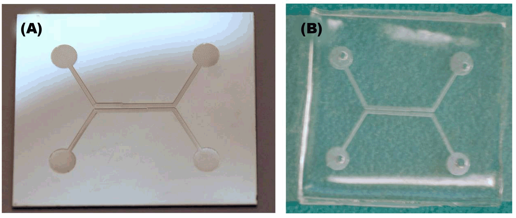
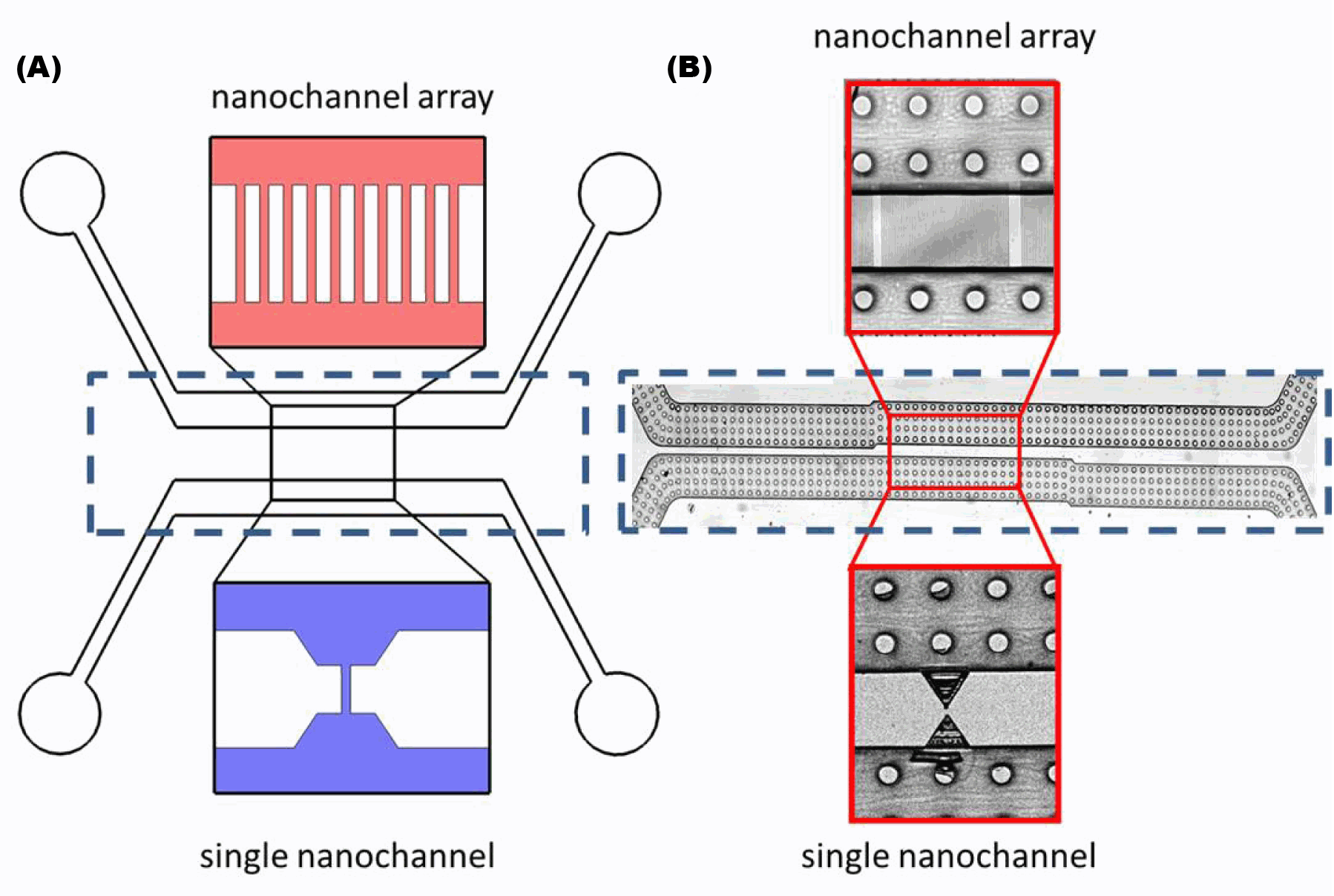
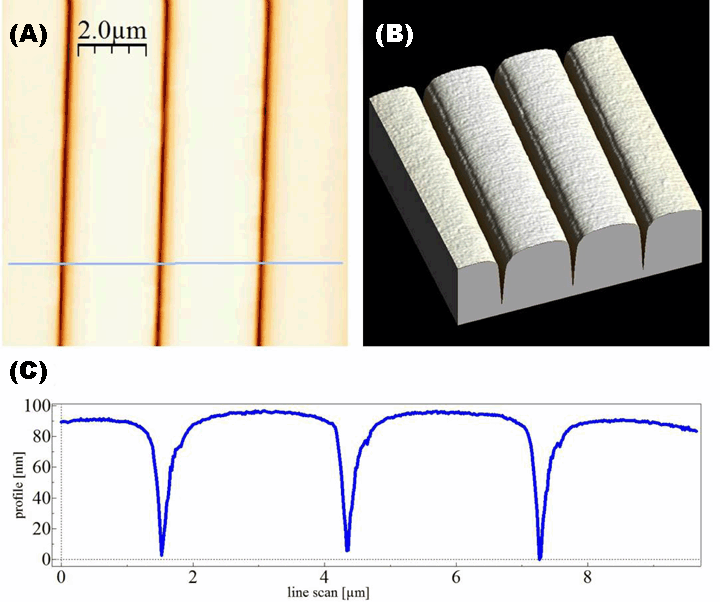
Two categories of polymers attracted the interest of researchers: elastomers, highly deformable materials, generally with a low Young's modulus enabling the recovery of their original shape upon removal of the applied strain, and thermoplastics, moldable materials if heated above a specific temperature, generally having high molecular weight and Young's modulus, thus resulting more brittle than elastomers. One of the most widespread elastomers is polydimethylsiloxane, while among thermoplastics, polymethymethacrylate (PMMA) is the most frequently used. [36] [37] [38] [39] The intensive use of PDMS for fabricating microfluidic systems is due to its interesting properties: it is optically transparent, chemically inert, non-toxic, gas permeable and non-flammable, but mainly it is well-suited for replica molding, a very cheap and simple technique to create an accurate replica even of the nanoscale features. These impressive characteristics significantly contributed to the extensive diffusion of PDMS bio-MEMS (biological MicroElectroMechanical Systems) or LOCs (Lab-On-a-Chips) for handling fluids in miniaturized devices, especially for biological applications. Our research group has developed an innovative technology to exploit the elastomeric nature of PDMS for fabricating tunable nanostructures with various and, if necessary, complex configurations: [24] single nanochannels, arrays of alternating deep and shallow structures, series of microstructures linked by nanochannels, etc. The versatility of this technology enables the creation of devices for various applications: sorting, biosensing and mapping. The fabrication process, described in Materials and Methods section, is based on a double REM procedure: a micromachined silicon mold is nanopatterned using a focused ion beam (FIB), then, upon the deposition of an anti-stiction layer, it is replicated using PDMS. This replica reproduces, in negative, micro and nanofeatures patterned on the master, therefore a second replication step is required to create a PDMS positive copy of the original silicon mold. Figure 1A shows a micromachined silicon mold of a device constituted of two facing U-shaped microchannels, each equipped with two circular reservoirs for fluids and electrodes insertion. Figure 1B shows the image of the PDMS positive replica obtained by applying the described procedure. As shown Figure 2A, different nanostructures can be patterned on the region between the microchannels in order to change the functionality of the device: arrays of nanochannels for sieving purposes, or a single nanochannel for biomolecule sensing. Figure 2B shows an optical image of a PDMS replica with the basic microfluidic layout. On the central area, indicated by the dashed rectangle, arrays of nanochannels (as those reported in the top inset) can be patterned to take advantage of DNA nanoconfinement effects for separating molecules of different length or, alternatively, a single nanochannel (similar to the one reported in the bottom inset) can be created for detecting biomolecule interactions with the nanostructure by monitoring ionic current variations. The final PDMS device, obtained by the second replication process, is exposed to an oxygen plasma treatment to activate the surface and bond it to a glass covering (typically a cover slip to optimally observe the nanostructures by optical microscopy). This oxygen plasma activation has a double function: changing the properties of the surface from hydrophobic to hydrophilic to fill nanostructures with aqueous solutions, and sealing irreversibly the device, to avoid liquid leaks. The obtained structures can be then used for biosensing and sieving experiments. However, the elastic properties of the used materials result to be extremely important for the development of advanced deformable devices, and they must be finely tuned in order to avoid problems of elastomeric collapse, but preserving the possibility of reversible deformation. Different formulations and procedures for PDMS preparation have been tested, with the aim of identifying the best characteristics for REM and nanostructure sealing. An efficient approach resulted to be the fabrication of composite devices made of a thin layer of h-PDMS, or of PDMS 3:1, and a thick layer of PDMS 10:1. This composition was successfully used to fabricate sub-100 nm high channels able to sustain a reversible mechanical deformation upon the application of an external load [24] or displacement, [40] as demonstrated by conductance measurements. Moreover, the method we use for nanostructure fabrication, based on FIB-patterning, led "naturally" to the creation of triangular structures of various aspect ratio and dimensions, which offer a good control of cross section size upon deformation. Figure 3A dipicts an atomic force microscopy image of the surface of a typical PDMS device containing an array of nanochannels. The 3D representation (Figure 3B) and the cross section profile (Figure 3C) allow to appreciate the triangular shape of the channels obtained by using the FIB nanopatterning based approach. This kind of triangular-shaped nanostructures are particularly interesting, due to their ability of inducing larger biomolecule extension relative to square or circular nanochannels of the same effective size, a great advantage for single molecule genomic mapping. To study the elongation of DNA strands in such nanoconfinement conditions, we performed Monte Carlo simulations of chains inserted in nanochannels of various dimensions and aspect ratios. [41] Our results, recently confirmed by Reinhart et al., show that entropic depletion occurs at the corners of triangular nanochannels, causing larger stretching of biomolecules compared to square or circular ones. [42] | ||||||
|
| ||||||
|
| ||||||
|
| ||||||
|
Discussion
| ||||||
|
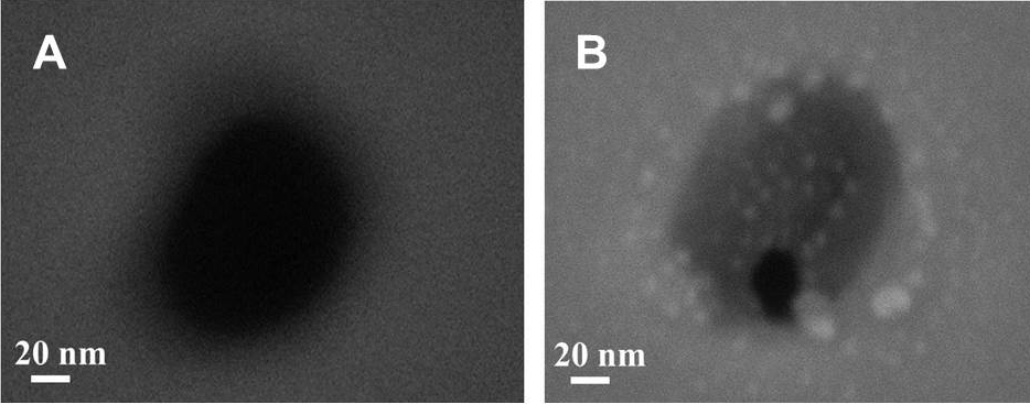
The triangular nanostructures offer not only higher confinement capabilities, but also a better control of their cross section size upon a mechanical stimulus. In order to better characterize the deformation of the structures upon the application of a mechanical stress, Finite Element Method (FEM) based numerical simulations were performed and compared with experimental measurements of ionic conductance. [43] They showed the pivotal role of the oxygen plasma treatment in creating an ultra-thin layer of nearly 100 nm on PDMS surface, whose high stiffness is essential both for device sealing and for reversibly tuning nanochannel dimensions during squeezing processes. All these advantages make our polymeric tunable nanochannel devices good candidates for the next generation high sensitivity biosensing applications. In fact, our experiments on DNA single molecule detection demonstrate that, applying a macroscopic mechanical compression to elastomeric nanostructures, it is possible to increase their confining power and vary the dynamics of DNA translocation process, [40] resulting in a longer time required for molecule passage. Thus, playing with the deformability of elastomeric materials is a simple but effective strategy to control molecule translocation across the sensing element and impart powerful and innovative manipulation capabilities to low cost devices. A further development of these nanostructured systems will be the exploitation of functionalization strategies to give selectivity and specificity to these systems. By now, surface modification of microfluidic structures is a well-established and widespread used strategy to enhance the functionalities of many categories of LOCs, thanks to the chemical selectivity offered by the immobilization of molecules on their surfaces. Surface modi?cation strategies are, generally, classified into physical adsorption and covalent modi?cation. Physical adsorption occurs when materials are adsorbed on the surface via hydrophobic or electrostatic interactions, while covalent modi?cations include molecules bounded to the surface. Many approaches both for hard material-based (Si, SiO2, Si3N4, etc.) and for polymeric (PDMS, PMMA, etc.) microfluidic platforms have been developed. [30] [31] The present challenge, however, concerns the development of functionalization procedures that allow to finely controlling the process of immobilization of probe molecules on the surface of the nanostructures, to simultaneously resize them and adapt their operation to a specific biological target. In our lab, Mussi et al. have recently exploited this approach for precisely tuning the characteristics of a nanopore drilled by a focused ion beam on a silicon nitride membrane. [29] The procedure uses an initial vapor-phase silanization whose duration regulates the final functionalization efficiency and thickness of the organic coating, thus controlling the final dimension of the nanostructure (see Materials and Methods). Figure 4(A-B) shows SEM images acquired on the same nanopore before, and after, respectively, the stable functionalization with oligonucleotides, following an initial 300 s vapor phase silanization step. The presence of the organic layer on the treated pore is associated to the appearance of a gray low-contrast internal area, well distinguished from the smaller dark residual open area. The use of the chemical functionalization thus allows to tune both the size and the functionality of the nanopore biosensor, without the need for a demanding nanofabrication technique. Furthermore, this method is applicable to different kind of couples of probe-target molecules, i.e. DNA, miRNA, high and low molecular weight proteins, even if an efficient application requires a careful evaluation of all the parameters influencing the process of chemical modification of surfaces in nanoconfined regions. Our current effort concerns the possibility to extend this approach to more complex deformable polymeric structures, in order to obtain adjustable and possibly reusable lab-on-chip devices for fast and low cost bioanalytics and diagnostics. | ||||||
| ||||||
|
Conclusion
| ||||||
|
Based on recent experimental results, we propose to combine two "tuning strategies" for the fabrication of deformable elastomeric biosensors whose selectivity is obtained by surface functionalization, and sensitivity is defined by nanoconfinement properties. These structures could offer the possibility of altering the dynamics of molecule passage, facilitating the collection of specific electrical and optical information on the target properties and its interaction with the nanostructure surface. The exploitation of this unique ability would allow sub-molecular analysis of nucleic acids, opening the way to the design and production of advanced next-generation sequencing tools. To achieve this goal, it will be necessary to integrate the skills and experience of researchers from different disciplines, applying a multidisciplinary approach which is essential to explore the future potential of Nanotechnology applied to Life Sciences. | ||||||
|
Acknowledgements
| ||||||
|
This work was supported by Italian Ministry of Education, University and Research with the National Project NANOMAX, the FIRB Project NEWTON and the Project ITALNANONET. | ||||||
|
References
| ||||||
| ||||||
|
[HTML Abstract]
[PDF Full Text]
|
|
Author Contributions:
Elena Angeli – Conception and design, Acquisition of data, Analysis and interpretation of data, Drafting the article, Critical revision of the article, Final approval of the version to be published Valentina Mussi – Conception and design, Acquisition of data, Analysis and interpretation of data, Drafting the article, Critical revision of the article, Final approval of the version to be published Paola Fanzio – Conception and design, Acquisition of data, Analysis and interpretation of data, Critical revision of the article, Final approval of the version to be published Chiara Manneschi – Analysis and interpretation of data, Critical revision of the article, Final approval of the version to be published Luca Repetto – Conception and design, Acquisition of data, Analysis and interpretation of data, Critical revision of the article, Final approval of the version to be published Giuseppe Firpo – Conception and design, Acquisition of data, Analysis and interpretation of data, Critical revision of the article, Final approval of the version to be published Patrizia Guida – Conception and design, Acquisition of data, Analysis and interpretation of data, Critical revision of the article, Final approval of the version to be published Vincenzo Ierardi – Conception and design, Acquisition of data, Analysis and interpretation of data, Critical revision of the article, Final approval of the version to be published Andrea Volpe – Analysis and interpretation of data, Critical revision of the article, Final approval of the version to be published Ugo Valbusa – Conception and design, Analysis and interpretation of data, Critical revision of the article, Final approval of the version to be published |
|
Guarantor of submission
The corresponding author is the guarantor of submission. |
|
Source of support
None |
|
Conflict of interest
Authors E.A., M.V., L.R., G.F., P.G., V.I. and U.V. declare a financial interest in the company (Nanomed Srl) attempting to commercialize the technology described in this manuscript. |
|
Copyright
© Elena Angeli et al. 2014; This article is distributed the terms of Creative Commons attribution 3.0 License which permits unrestricted use, distribution and reproduction in any means provided the original authors and original publisher are properly credited. (Please see Copyright Policy for more information.) |
|
|